|
Product Details:
Payment & Shipping Terms:
|
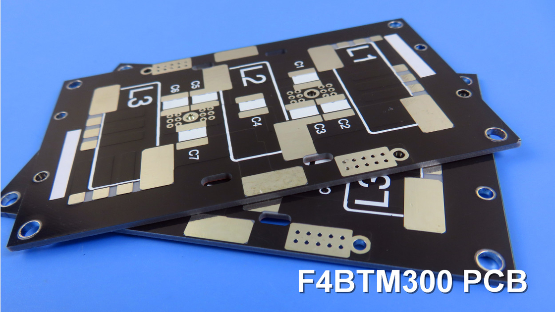
| Material: | F4BTM450 Core | PCB Size: | 63mm X 63 Mm=1PCS, +/- 0.15mm |
|---|---|---|---|
| Copper Weight: | 1oz (1.4 Mils) Outer Layers | Surface Finish: | Immersion Gold |
| Layer Count: | 2-layer | PCB Thickness: | 3.2mm |
| Highlight: | Black Soldermask F4BTM PCB,Immersion Gold F4BTM PCB,3.2mm F4BTM PCB |
||
Introducing our newly shipped PCB based on F4BTM. This series of advanced circuit laminates combines a glass fiber cloth, nano-ceramic filling, and polytetrafluoroethylene resin, meticulously prepared using scientific techniques and rigorous pressing processes.
The F4BTM PCB series builds upon the F4BM dielectric layer, incorporating high-dielectric and low-loss nanoscale ceramics. This unique composition provides numerous benefits, including:
1. Enhanced Performance:
- Higher Dielectric Constant (Dk):
Achieve superior signal transmission with a Dk of 4.5 at 10 GHz, enabling efficient high-frequency operation.
- Low Dissipation Factor:
Experience minimal signal loss with a dissipation factor of 0.002 at 10 GHz, ensuring optimal performance in demanding applications.
- Improved Thermal Stability:
The F4BTM PCB exhibits a low coefficient of thermal expansion (CTE) with values of 10 ppm/°C (X-axis), 12 ppm/°C (Y-axis), and 51 ppm/°C (Z-axis) within the temperature range of -55°C to 288°C. This exceptional thermal stability ensures reliable performance under extreme temperature conditions.
- Consistent Dielectric Constant over Temperature:
Benefit from a low thermal coefficient of Dk at -60 ppm/°C within the temperature range of -55°C to 150°C, allowing for consistent signal integrity across varying thermal environments.
- Excellent Moisture Resistance:
With a moisture absorption rate of 0.05%, the F4BTM PCB offers exceptional resistance to moisture, ensuring long-term reliability even in humid conditions.
| Product Technical Parameters | Product Models & Data Sheet | ||||||
| Product Features | Test Conditions | Unit | F4BTM298 | F4BTM300 | F4BTM320 | F4BTM350 | |
| Dielectric Constant (Typical) | 10GHz | / | 2.98 | 3.0 | 3.2 | 3.5 | |
| Dielectric Constant Tolerance | / | / | ±0.06 | ±0.06 | ±0.06 | ±0.07 | |
| Loss Tangent (Typical) | 10GHz | / | 0.0018 | 0.0018 | 0.0020 | 0.0025 | |
| 20GHz | / | 0.0023 | 0.0023 | 0.0026 | 0.0035 | ||
| Dielectric Constant Temperature Coefficient | -55 º~150ºC | PPM/℃ | -78 | -75 | -75 | -60 | |
| Peel Strength | 1 OZ F4BTM | N/mm | >1.6 | >1.6 | >1.6 | >1.6 | |
| 1 OZ F4BTME | N/mm | >1.4 | >1.4 | >1.4 | >1.4 | ||
| Volume Resistivity | Standard Condition | MΩ.cm | ≥1×10^7 | ≥1×10^7 | ≥1×10^7 | ≥1×10^7 | |
| Surface Resistivity | Standard Condition | MΩ | ≥1×10^6 | ≥1×10^6 | ≥1×10^6 | ≥1×10^6 | |
| Electrical Strength (Z direction) | 5KW,500V/s | KV/mm | >26 | >30 | >32 | >32 | |
| Breakdown Voltage (XY direction) | 5KW,500V/s | KV | >34 | >35 | >40 | >40 | |
| Coefficientof Thermal Expansion | XY direction | -55 º~288ºC | ppm/ºC | 15,16 | 15,16 | 13,15 | 10,12 |
| Z direction | -55 º~288ºC | ppm/ºC | 78 | 72 | 58 | 51 | |
| Thermal Stress | 260℃, 10s,3 times | No delamination | No delamination | No delamination | No delamination | ||
| Water Absorption | 20±2℃, 24 hours | % | ≤0.05 | ≤0.05 | ≤0.05 | ≤0.05 | |
| Density | Room Temperature | g/cm3 | 2.25 | 2.25 | 2.20 | 2.20 | |
| Long-Term Operating Temperature | High-Low Temperature Chamber | ℃ | -55~+260 | -55~+260 | -55~+260 | -55~+260 | |
| Thermal Conductivity | Z direction | W/(M.K) | 0.42 | 0.42 | 0.50 | 0.54 | |
| PIM | Only applicable to F4BTME | dBc | ≤-160 | ≤-160 | ≤-160 | ≤-160 | |
| Flammability | / | UL-94 | V-0 | V-0 | V-0 | V-0 | |
| Material Composition | / | / | PTFE, Fiberglass Cloth, nano-ceramics F4BTM paired with ED copper foil, F4BTME paired with reverse-treated (RTF) copper foil. |
||||
2. Versatile PCB Construction:
- 2-Layer Rigid PCB:
This PCB is a 2-layer rigid PCB, providing a robust foundation for your high-frequency designs.
- Superior Build Quality:
Featuring 35 μm copper layers on both the top and bottom sides and a 3.05 mm (120 mil) F4BTM450 core, this PCB offers excellent electrical conductivity and structural integrity.
- Precise Specifications:
The board dimensions measure 63 mm x 63 mm with a tolerance of +/- 0.15 mm, providing ample space for your circuitry. The minimum trace/space is 6/8 mils, and the minimum hole size is 0.4 mm, enabling intricate and compact designs.
- Reliable Plating and Surface Finish:
This RF PCB includes 20 μm via plating thickness for reliable interconnection. It is finished with an immersion gold surface finish, ensuring superior conductivity and protection against oxidation.
- Rigorous Quality Assurance:
Each PCB undergoes a comprehensive 100% electrical test prior to shipment, guaranteeing optimal functionality and performance.
| PCB Material: | PTFE / glass fiber cloth / Nano-ceramic filler | ||
| Designation (F4BTM ) | F4BTM | DK (10GHz) | DF (10 GHz) |
| F4BTM298 | 2.98±0.06 | 0.0018 | |
| F4BTM300 | 3.0±0.06 | 0.0018 | |
| F4BTM320 | 3.2±0.06 | 0.0020 | |
| F4BTM350 | 3.5±0.07 | 0.0025 | |
| Layer count: | Single Sided, Double Sided PCB, Multilayer PCB, Hybrid PCB | ||
| Copper weight: | 0.5oz (17 µm), 1oz (35µm), 2oz (70µm) | ||
| Dielectric thickness (or overall thickness) | 0.25mm, 0.508mm, 0.762mm, 0.8mm, 1.0mm, 1.016mm, 1.27mm, 1.524mm, 2.0mm, 3.0mm, 4.0mm, 5.0mm, 6.0mm, 8.0mm, 10.0mm, 12.0mm | ||
| PCB size: | ≤400mm X 500mm | ||
| Solder mask: | Green, Black, Blue, Yellow, Red etc. | ||
| Surface finish: | Bare copper, HASL, ENIG, Immersion silver, Immersion tin, OSP, Pure gold, ENEPIG etc.. | ||
![]()
3. Wide Range of Applications:
The F4BTM PCB is suitable for various applications, including:
- Aerospace Equipment, Space, and Cabin Equipment
- Microwave and RF Systems
- Radar and Military Radar Systems
- Feed Networks
- Phase-Sensitive Antennas and Phased Array Antennas
- Satellite Communications
4. Global Availability and Quality Standards:
The F4BTM PCB is available worldwide, enabling you to access this advanced technology regardless of your location. It adheres to the IPC-Class-2 quality standard, ensuring high-quality manufacturing and consistent performance.
Unlock the potential of high-frequency circuitry with the F4BTM PCB. Experience unrivaled performance, outstanding reliability, and unparalleled design flexibility for your cutting-edge electronic projects.
![]()
Contact Person: Ms. Ivy Deng
Tel: 86-755-27374946
Fax: 86-755-27374848