|
Product Details:
Payment & Shipping Terms:
|
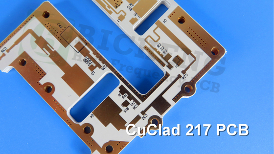
| Material: | CuClad 217 Core | PCB Size: | 106.8mm X 51.8 Mm=1PCS, +/- 0.15mm |
|---|---|---|---|
| Copper Weight: | 1oz (1.4 Mils) Outer Layers | Surface Finish: | Immersion Silver |
| Layer Count: | 2-layer | PCB Thickness: | 0.3mm |
| Highlight: | 217 PCB,10mil CuClad PCB,Immersion Silver PCB |
||
Introducing the CuClad 217 PCB, a newly shipped product that harnesses the advanced features of Rogers CuClad 217 laminates. Meticulously engineered, these laminates combine cross-plied, woven fiberglass with precisely controlled PTFE composites. The CuClad 217 PCB stands out with its impressive performance, offering a low dielectric constant (Dk) of 2.17 or 2.20. Its cross-plied construction ensures electrical and mechanical isotropy within the plane, resulting in enhanced signal propagation and superior signal-to-noise ratios.
Key Features:
Dielectric Constant: DK 2.17 or 2.2 at 10GHz / 1MHz
Dissipation Factor: 0.0009 at 10GHz
Low Moisture Absorption: 0.02%
Strong Peel Strength: 14 lbs/in
Low Outgassing: Total Mass Loss (TML) 0.01%, Collected Volatile Condensable Material (CVCM) 0.01%, 0 Water Vapor Regain (WVR)
Cross-Plied Woven Fiberglass with High PTFE to Glass Ratio
Improved Dielectric Constant Uniformity
Benefits:
Stable Dk over a wide frequency range
Allows wider line widths for lower insertion loss
Low circuit losses at high frequencies
Improved dimensional stability for design flexibility
Enables meeting strict specifications
Electrical and mechanical isotropy in the X-Y plane
Ideal for circuits sensitive to variations in dielectric constant
![]()
Featuring a 2-layer rigid stackup, the CuClad 217 PCB consists of a 35 μm copper layer, a 0.254 mm (10mil) Rogers CuClad 217 core, and another 35 μm copper layer.
It comes in precise board dimensions of 106.8mm x 51.8mm (1PCS) with a tolerance of +/- 0.15mm. The PCB supports a minimum trace/space of 6/5 mils and a minimum hole size of 0.35mm. It does not include blind vias. With a finished board thickness of 0.3mm and a finished copper weight of 1oz (1.4 mils) on the outer layers, the CuClad 217 PCB ensures optimal performance. It features a 20 μm via plating thickness and an immersion silver surface finish for excellent conductivity and corrosion resistance.
The PCB does not include top or bottom silkscreen or solder mask. Each PCB undergoes a rigorous 100% electrical test before shipment to ensure optimal functionality.
With 27 components and a total of 103 pads, including 78 through-hole pads and 25 top surface mount technology (SMT) pads, the CuClad 217 PCB offers ample flexibility for various designs. It features 15 vias and 2 nets, enabling efficient signal routing and connectivity.
It meets the IPC-Class-2 quality standards, the CuClad 217 PCB guarantees high-quality performance and reliability. It is available for shipping worldwide, allowing customers from various locations to experience its exceptional features.
The CuClad 217 PCB finds applications in a range of fields, including radars, electronic countermeasures, electronic support measures, and microwave components such as LNAs, filters, and couplers. Its superior properties make it an ideal choice for demanding electronic applications that require high performance and reliability.
![]()
Contact Person: Ms. Ivy Deng
Tel: 86-755-27374946
Fax: 86-755-27374848